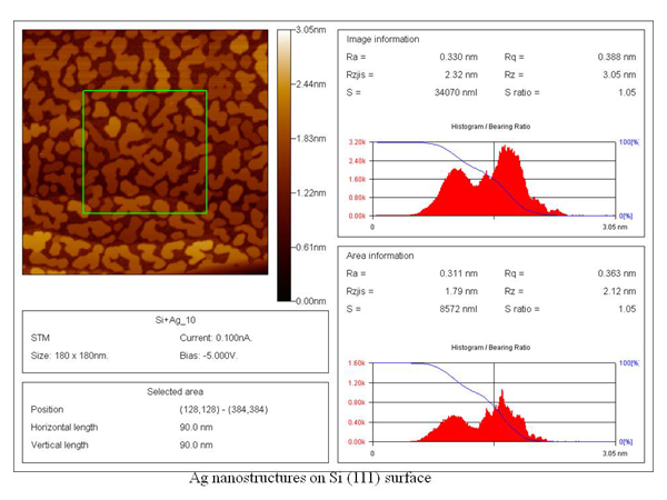
The image shows silver (Ag) nanostructures deposited on the surface of silicon (Si)
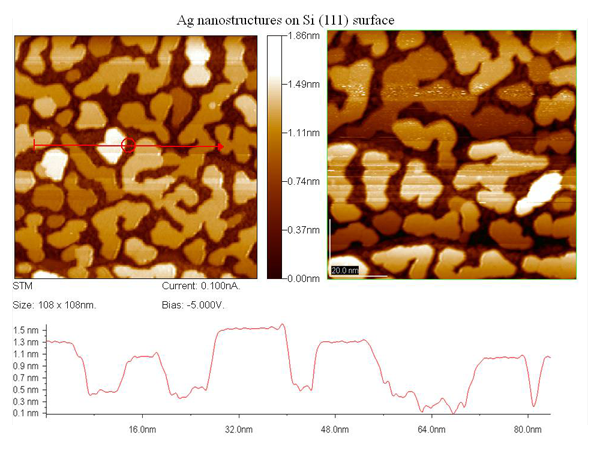
Silver (Ag) nanostructures deposited on a silicon (Si) surface The bottom graph shows a cross-section of the surface along the red line marked in the image. The graph shows the change in relief heights, allowing us to estimate the shape and size of the nanostructures).
The image shows silver (Ag) nanostructures formed on a silicon (Si) surface with orientation (111) Main details: Left image: The scanning area is 63.5 × 63.5 nm².
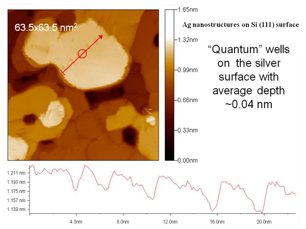
The image shows ‘quantum wells’ on the surface of silver (Ag) formed on a silicon substrate (Si(111)). Main details: Left image: The scanning area is 63.5 × 63.5 nm². The red arrow indicates the area for which the linear height profile was taken.
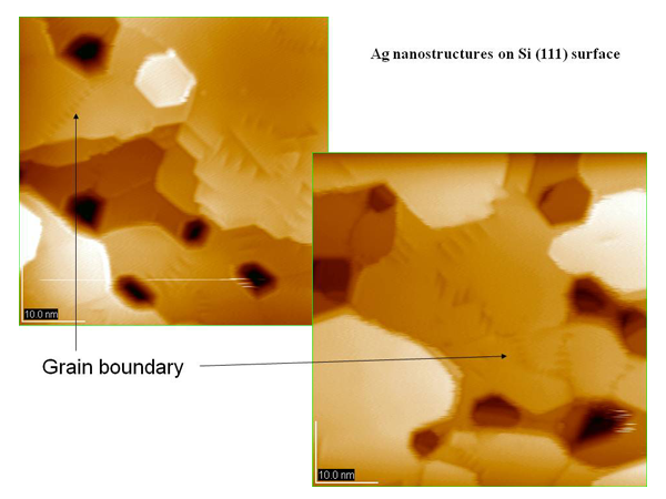
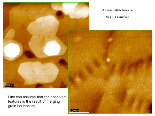
The photo shows the surface images of silver (Ag) nanostructures placed on a silicon (Si) substrate with orientation (111). The grain structure of the surface with noticeable grain boundaries, as well as individual nanostructures, are visible.
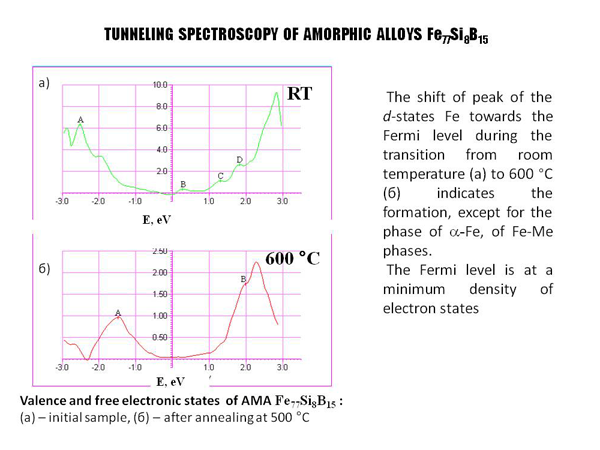
The image shows the results of tunneling spectroscopy of amorphous alloys
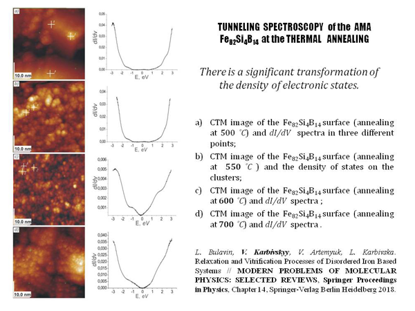
The image shows the results of a tunneling spectroscopy study of an amorphous alloy during thermal annealing. The study focuses on the change in the density of electronic states at different temperatures.
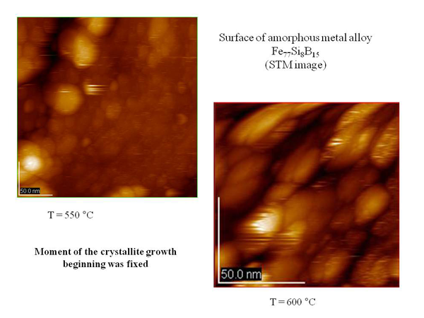
The image shows scanning tunneling microscopic (STM) images of the surface of an amorphous metal alloy at different thermal annealing temperatures.
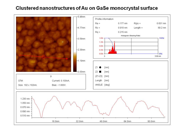
The image shows gold (Au) nanostructures deposited on the surface of a GaSe single crystal, obtained by scanning tunneling microscopy (STM).
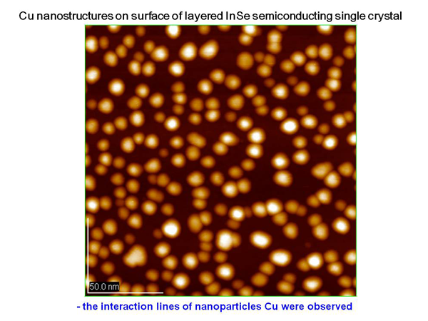
The image shows copper (Cu) nanostructures formed on the surface of a layered InSe semiconductor single crystal.
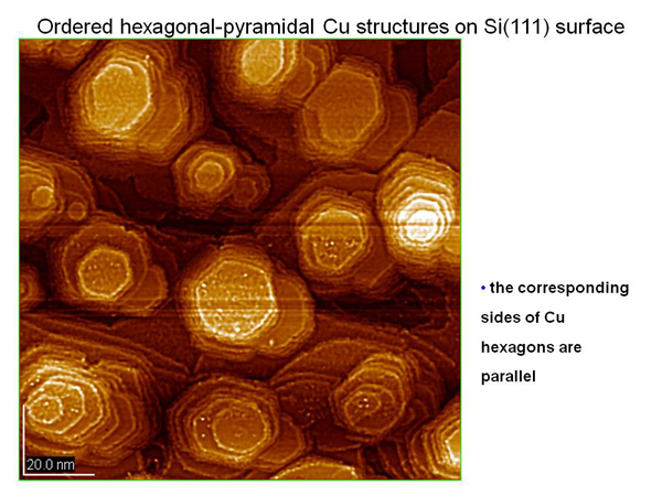
The image shows the ordered hexagonal pyramidal structures of copper (Cu) formed on the Si(111) silicon surface.
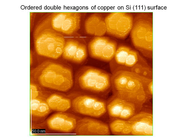
The image shows ordered double hexagonal copper (Cu) nanostructures formed on the Si(111) silicon surface.
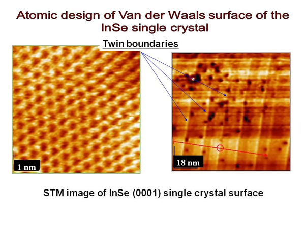
Atomic surface structure of InSe (0001) single crystal obtained by STM. Features: Twin boundaries, which are defects in the structure, are indicated. The image shows the atomic topography with high resolution.
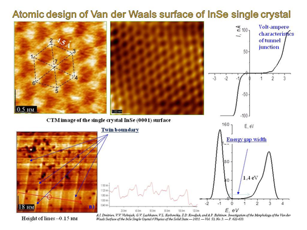
Investigation of the electronic structure of the InSe (0001) surface. Features: The density of states (DOS) distribution and the energy gap width obtained by tunneling spectroscopy are shown. The spatial arrangement of atoms is possibly also illustrated.
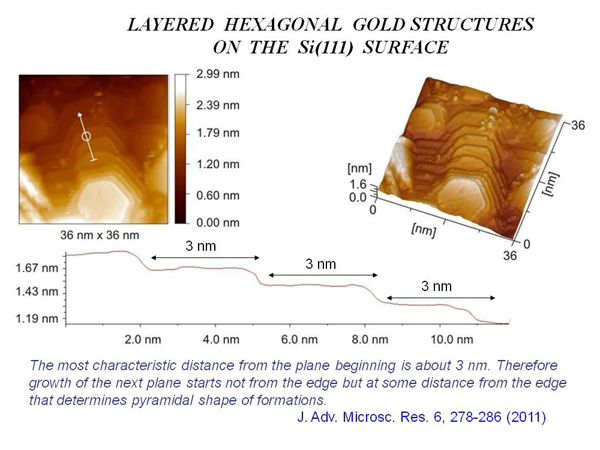
Hexagonal gold nanostructures on Si(111) surface. Features: The topography is presented with a focus on the multilayers and the characteristic layer spacing (~3 nm)
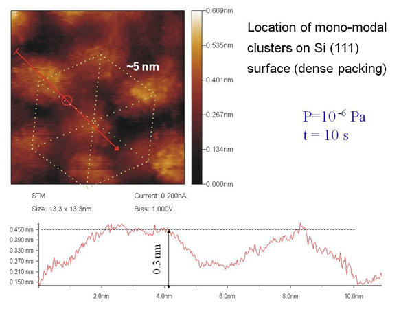
Monocluster formations on the surface of Si(111). Features: Dense packing of clusters with indication of their location and height (~0.3 nm).
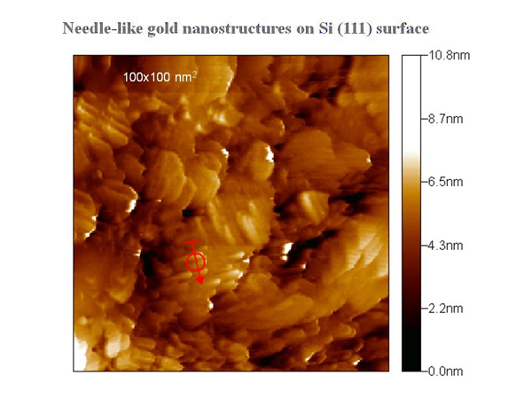
Needle-like gold nanostructures on the surface of Si(111). Features: The image shows high anisotropy and cluster distribution with height and area detail.
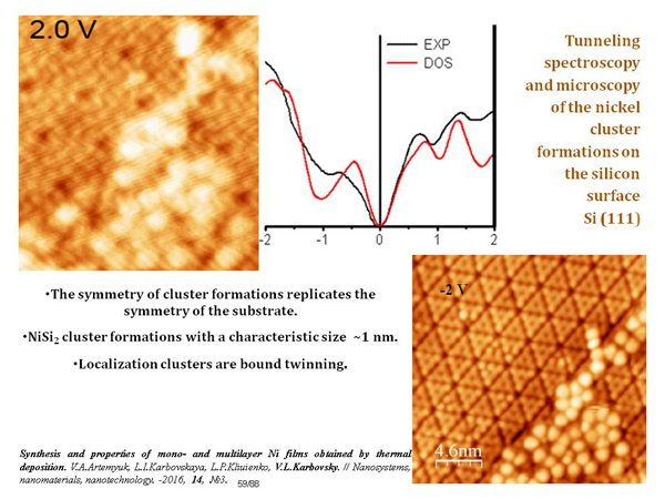
Nickel clusters on the surface of Si(111) obtained by tunneling spectroscopy. Features: Synchronisation of the clusters with the substrate symmetry, localisation due to twin formation mechanisms.
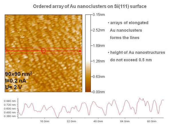
Ordered arrays of gold nanoclusters on the surface of Si(111).
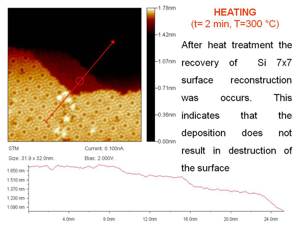
Heating of the Si(111) surface and restoration of the 7×7 reconstruction.
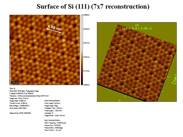
Reconstruction of Si(111) surface in 7×7 format.